
LinkRF
EME and Weak signal communication



Copyright © 2008-2026, Eich Switzerland by Alex Artieda, HB9DRI


DRI-X4W
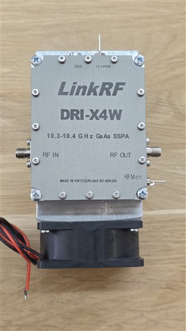
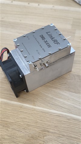
DRI-X4W
10 GHz 4W Solid-State Power Amplifier (SSPA)
PHASE 1 DRI-XSeries as a driver for PHASE 2 DRI-X25W
Technical Product Specification
1. Key Features
- Semiconductor Technology: Gallium Arsenide (GaAs) FET
- Frequency Range: 10.3 to 10.5 GHz (Optimized 10.368 Ghz)
- High Linearity: Designed for high data-rate digital modulation schemes, Digital, CW and SSB
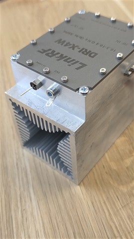
- Thermal Management: Integrated aluminium chassis housing with highly efficient heat dissipation properties
2. Electrical Specifications
All specifications are verified at an ambient room temperature of 22°C with a regulated DC supply voltage of 10.43 VDC.
Parameter
|
Speification
|
Unit
|
Notes / Condition
|
Operative Frec.
|
10.368
|
GHz
|
Fixed Test Frec.
|
Linear Small signal Gain
|
15.1
|
dB
|
mesure at Pin=133mW
|
Output Power P1dB
|
4.66 / +36.7
|
W / dBm
|
Exact 1dB compression point
|
Input Power P1dB
|
0.186 / +22.62
|
W / dBm
|
Required drive for P1dB
|
Saturated Output Power
|
5.05 / +37.03
|
W / dBm
|
Maximum deep Saturation limit
|
Power Added Efficiency PAE
|
34.4 / 41.1
|
%
|
Measured at P1dB / Full Sat.
|
Drain Efficiency
|
35.7 / 43.2
|
%
|
Measured at P1dB / Full Sat
|
Gain Flatness /Slump short
|
-0.04
|
dB
|
20 minute continuous key down test
|
Gain Flatness /Slump Long
|
-0.08
|
dB
|
12 hours continuous key down test
|
3. DC & Power Supply Requirements
Parameter
|
Specification
|
Unit
|
Notes / Conditions
|
Operating Drain Voltage
|
10.43
|
VDC
|
Regulated DC supply voltage
|
Quiescent current Idq
|
0.85
|
A
|
Zero RF input drive applied
|
Operating current Id
|
1.12 to 1.28
|
A
|
Dynamic range from peak saturation to hot level 0
|
Maximum current Consumption
|
1.28
|
A
|
Peak current during thermal heat soak
|
4. Thermal & Environmental Specifications
Parameter
|
Specification
|
Unit
|
Notes / Condition
|
Thermal Dissipation
|
13.35
|
W
|
Continuous thermal reject load to heatsink under full RF drive
|
Enclousure to Heatsink Temp.
|
28.3
|
°C
|
Measure at chasis junction with ambient temp 24.4 °C
|
Heatsink Thermal Resistance
|
0.26
|
°C/W
|
Enclosure to air thermal pathway capacity with multifins tunnel dissipator heatsink
|
Estimated Die Junction Temperature
|
116.3
|
°C
|
Calculated based on the standard GaAs packaging
|
Maximum Rated Junction Temp Tch
|
175
|
°C
|
Absolute maximum rating for GaAs transistor reliability
|
Thermal Desing Margin
|
58.7
|
°C
|
Headroom remaining under worst case continuous wave (CW) soak
|
5. Engineering Summary for long life operation
- Heatsink Performance: The thermal resistance 0.26 °C/W due to the efficiency of the wind-tunnel design with multifins allowa rapid heat dissipation.
- Junction Temperature Room: Even with the quieter, lower-airflow fan, your true internal die junction temperature sits comfortably at 116.3°C, providing
a massive 58.7°C margin below the device's real 175°C failure point.
