
LinkRF
EME and Weak signal communication



Copyright © 2008-2026, Eich Switzerland by Alex Artieda, HB9DRI


DRI-X25W
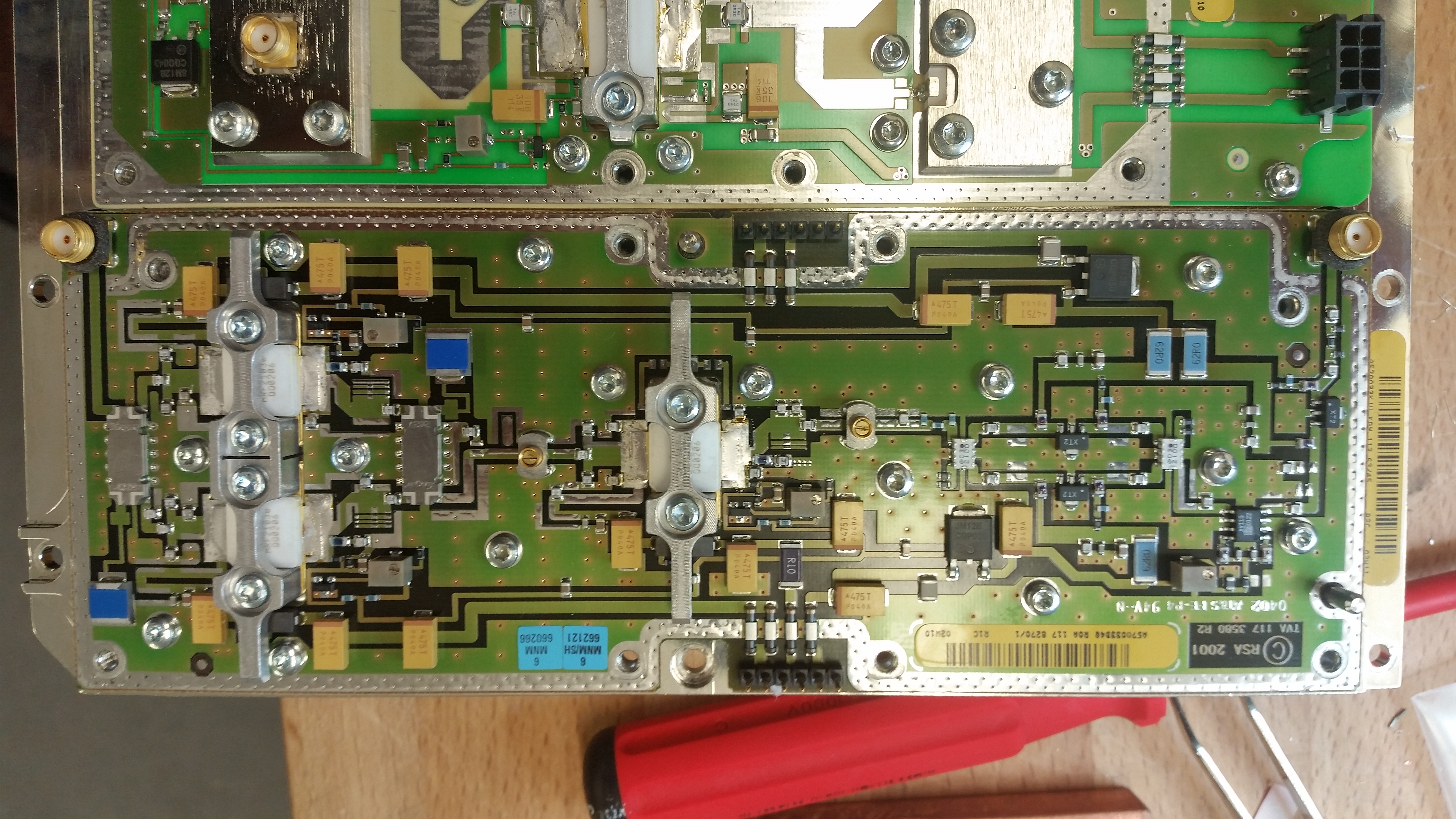
The DRI-XSeries is a modular family of GaAs — Gallium Arsenide solid-state power amplifiers developed specifically around 10.368 GHz weak-signal and EME operation.
The first product, DRI-X4W, is both a complete 4–5 W EME amplifier and the driver platform for the forthcoming DRI-X25W. The longer-term architecture allows higher RF power to be obtained by combining independent amplifier modules rather than concentrating the entire station power in one very expensive semiconductor.
The central idea is to have a "affordable" battle horse modular pallet producing 25W to later combine 2,3,4,or 5 25W pallets using phase rersonance cavities (silver plated) to obtain as much less IL in the combining process. As a matter of fact if properlly interconection is provided 4 DRI-X25W will produce minumum 90 watts of effective power with a WR-90 output direct into the wave guide antenna relay
To desing a modular pallet many central topics become "problematic", the selection of the device: GaAs vs GaN, the properly pcb and the way is design and grounded in the enclosure, the enclosure per se with negative resonance problematic almost ignored by the amateur builders, last at not least a properly electronics to manage specially the temperature and Id based on a MCU insted of simple analog circuits.
Contrary to most of the ham radio desings, where a single pcb host 2 to 3 active devices, branch line combiners and the full electronic to regulate the Vd and Vg, the DRI-X25W looks like that:
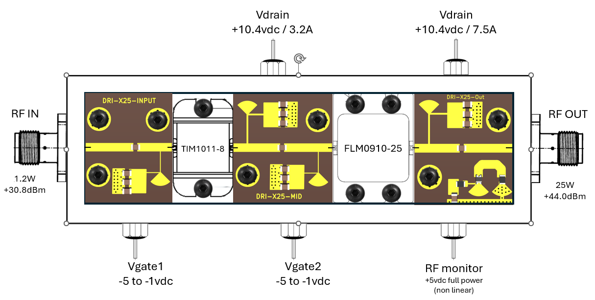
The internal cavity is just 96.2mm x 25mm x 12mm and it was desing using the RESOBOX software, a propietary software desing by my self to analyse resonance point in the TE and TM fields, the DRI-X4W was desing using my software and when I close the lid the SSPa increasi his power by 5% aprox, contrary to many amateur desing where misterious resonace are not in consideration, closing the enclouser always give you 10 to 40% less power, forcing you to use "RF abosrber material" to compensate the poor enclosure desing.
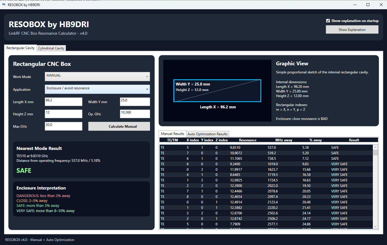
As you see in the previous picture the propose cavity for the DRI-X25W will have resonace points at 5.18% and 5.20% away from 10.368 GHz, the minImum practical separation must be at leat 2.8% otherwise you will have oscillations and low power when you close the enclosure, forcing you to use RF absorber materials with not 100% good results.
The DRI-X25W is in the final stage and I hope to publish my first practical results in 5 to 6 weeks aprox. PCB are ready and now is a mater to buid, the CNC enclosure,and present all parts inside.
MORE TO COME!!

DRI-XPS-25W
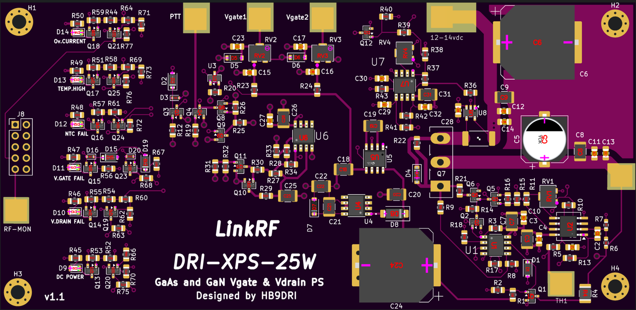
DRI-XPS-25W — Intelligent Vdrain & Vgate Power Supply and Protection System
**Work in Progress — LinkRF / HB9DRI**
The **DRI-XPS-25W** is a dedicated power-supply, sequencing, protection and monitoring controller developed for the **DRI-X25W 10 GHz GaAs SSPA**, using a TIM1011 driver and FLM0910-25L final amplifier.
The same circuit will be used in the DRI-X50W (10GHz 50W SSPA under development) wiht minor adaptations.
Can be easy modify to work with GaN devices with Vdrain voltages from 18 to 32 vdc and current up to 15amps
Unlike a conventional DC regulator, the DRI-XPS-25W has been designed around the particular requirements of high-power **GaAs /GaN FET microwave amplifiers**, where correct gate/drain sequencing and rapid protection are essential. The system controls both the negative gate supplies and the high-current drain supply, continuously supervises the important operating conditions, and immediately removes Vdrain when an unsafe condition is detected.
The first fully assembled prototype PCBs are presently in production. Hardware commissioning and characterization will follow.
Main characteristics
* **Input supply:** 12–14 VDC
* **Regulated Vdrain:** approximately **10.5 VDC**
* Designed for approximately **12 A operating current**, with adjustable overcurrent protection
* High-current **P-channel MOSFET linear regulator**
* Independent adjustable **Vgate1 and Vgate2 negative bias outputs**
* Raw negative supply generated locally from the main DC input
* Automatic **Vgate-before-Vdrain startup sequencing**
* Controlled shutdown with **Vdrain removed before negative gate bias disappears**
* PTT-controlled Vdrain**, avoiding unnecessary PA idle dissipation
* Automatic shutdown if the negative gate supply fails
* Temperature monitoring directly at the power FET
* NTC sensor open-circuit and abnormal-temperature protection
* Adjustable temperature shutdown, presently designed around **60–65 °C FET case temperature**
* High-side current measurement
* Adjustable **latched overcurrent protection**
* Active Vdrain output discharge
* Local status indication
* Six logic-level monitoring outputs for the forthcoming digital control system
* Four-layer PCB implementation
Vdrain regulation
The high-current drain supply is regulated to approximately **10.5 V** from a nominal 12–14 V station supply.
A high-current **IXYS IXTH52P10P P-channel MOSFET** is used as the series pass device. The MOSFET is mounted externally on the main heatsink through a copper heat spreader, allowing the considerable regulator dissipation to be transferred directly to the cooling system.
A precision **TL431 2.495 V reference** and operational-amplifier control loop regulate the drain voltage. The regulator has deliberately been implemented as a linear system rather than a switching converter, avoiding the generation of additional switching products close to a very sensitive microwave/EME receiving and transmitting environment.
Dual negative Vgate supplies
The two GaAs devices require independent negative gate-bias adjustments. The DRI-XPS-25W therefore provides separate:
**Vgate1** — for the driver stage
**Vgate2** — for the final stage
An LT1054 charge-pump circuit generates the negative supply, followed by individually adjustable and filtered gate-bias networks.
The negative gate supply is not merely another auxiliary voltage. It forms part of the PA protection system. The controller continuously supervises it, and **Vdrain cannot be enabled unless the negative gate supply is present and healthy**.
This is particularly important with GaAs / GaN FETs: loss of negative gate bias while drain voltage remains applied could result in excessive drain current and potentially destroy the device.
Automatic power sequencing
The DRI-XPS-25W includes dedicated hardware sequencing.
At power-up, the negative gate supply is established first. Only after the gate-bias system has stabilized does the sequencer permit the 10.5 V Vdrain supply to become active.
The reverse sequence is enforced during shutdown. Vdrain is switched off and actively discharged while the negative gate supply remains available for a controlled hold-up period.
The design therefore follows the fundamental GaAs PA rule:
**POWER ON:** Vgate - delay - Vdrain
**POWER OFF:** Vdrain OFF - discharge - Vgate OFF
The sequencing is implemented in hardware and does not depend on software or an MCU.
PTT operation
The PA does not need to remain at its full quiescent drain current while receiving.
A simple **PTT-to-GND input** enables the drain supply. With PTT released, Vdrain is inhibited while the negative gate system remains correctly biased.
This reduces unnecessary dissipation in the amplifier and simplifies integration with the transceiver or station-control system.
Temperature protection
A **10 kO NTC sensor** is mounted in the aluminium immediately adjacent to the FLM0910-25L power device.
The controller monitors this sensor independently of any future MCU. If the power-device temperature exceeds the preset threshold—initially approximately **60–65 °C at the case**—Vdrain is immediately inhibited.
The sensor itself is also supervised. An **open NTC connection produces a shutdown**, while a shorted sensor is interpreted as an excessive-temperature condition. A broken sensor wire therefore cannot silently disable the thermal protection.
High-current monitoring and latched protection
Drain current is measured on the high side using a **5 mO current shunt and INA293 current-sense amplifier**.
The present scaling is approximately:
** 1. A = 0.1 V**
**10 A = 1.0 V**
**12 A = 1.2 V**
An independent hardware comparator provides adjustable overcurrent protection. Once an overcurrent event occurs, the system enters a **latched shutdown condition** rather than repeatedly cycling the PA on and off into a possible fault.
Normal operation is restored by the intended reset/power-cycle procedure.
The initial trip point will be established during prototype characterization. It is intentionally adjustable so that the final setting can be based on the measured current at RF compression rather than an arbitrary fixed value.
Central hardware protection — KILL
The different protection circuits converge on a common hardware shutdown function. Vdrain is inhibited if any critical condition is detected, including:
* PTT inactive
* Negative Vgate supply failure
* Excessive temperature
* NTC sensor failure
* Overcurrent
* Startup sequencing incomplete
The important point is that **none of these fundamental protections depends on firmware**. Even if the future MCU, communication system or remote-control software fails, the primary SSPA protection remains operational.
Active Vdrain discharge
Simply switching off a high-current regulator does not necessarily remove drain voltage immediately because the output capacitors contain stored energy.
The DRI-XPS-25W therefore incorporates an **active VOUT discharge circuit**. When Vdrain is disabled, the output capacitance is deliberately discharged so that the GaAs / GaN devices do not remain exposed to a slowly decaying drain supply.
I want to emphasis the importance of the "Active Drain Discharge", conventional amateur PS desing used in GaAs and GaN dont have this protection, then every power cycle turn as a "SILENT KILLER" for fractions of seconds the FET is expose to Vdrain when Vgate already dissapear; the consequence is a slow but steady deterioration of the FET characteristics
This function will be characterized with an oscilloscope during prototype testing together with the Vgate hold-up timing.
Local monitoring
The first hardware version provides local indication of six important operating conditions:
**DC POWER — VDC DRAIN — VDC GATE FAIL — NTC FAIL — TEMPERATURE — OVER CURRENT**
The same information is also made available as **3.3 V logic signals** for the next development stage.
Phase 2 — Remote monitoring and control
The second development phase is already under way.
An MCU-based interface will provide complete remote supervision and control of the SSPA. The power amplifier may be installed outdoors close to the antenna, while the operator and radio equipment can be located a considerable distance away.
Communication between the local and remote controllers is planned using **RS-485 over a twisted pair**, allowing cable distances of **up to approximately 1 km** under suitable installation and data-rate conditions.
The architecture uses two controllers:
**Station / Radio side MCU -- RS-485 twisted pair -- SSPA-side MCU -- DRI-XPS-25W / SSPA**
PTT originates at the radio/station side. The local controller transmits the command over RS-485 to the MCU installed inside the SSPA enclosure, which then controls the PA PTT input.
The SSPA-side controller will also read the six hardware status outputs and return operating information to the station.
The intention is to provide remote indication and control of parameters such as **DC power status, Vdrain status, Vgate failure, NTC failure, overtemperature and overcurrent**, with provision for further telemetry as development continues.
Crucially, the MCU is an **additional supervisory layer**, not the primary protection system. Gate-failure, thermal, overcurrent and sequencing protection remain implemented directly in hardware on the DRI-XPS-25W.
RF Power Monitoring — RF_MON
The remote monitoring system will also include **RF_MON**, providing real-time indication of the SSPA RF output power.
A directional RF detector associated with the SSPA output produces a **DC voltage proportional to the detected RF power**. This analog `RF_MON` voltage will be measured by the SSPA-side MCU and transmitted over the RS-485 link to the station-side controller.
During final SSPA characterization, the RF detector will be calibrated against accurately measured output power. A **calibration/mapping table** will then relate the measured detector voltage to actual RF output power, for example:
**RF_MON voltage -- calibrated RF output power in watts**
Because the detector response is not assumed to be perfectly linear, the MCU can use the calibration table with interpolation between measured points rather than relying on a simple voltage-to-power conversion factor.
This will allow the station-side display to show the **actual calibrated relative/forward RF output power in watts**, together with the existing DC power, Vdrain, Vgate failure, NTC failure, temperature and overcurrent status information.
The RF_MON function is intended primarily for **operational power monitoring**, with its final accuracy and calibration range to be established during RF testing of the completed DRI-X25W amplifier.
Current project status — September 2026
The schematic and four-layer PCB design are complete. KiCad Design Rules Check currently reports:
0 Errors — 0 Warnings — 0 Unconnected Items
Two fully assembled prototype boards are presently in production. Once received, both units will undergo an identical step-by-step commissioning program covering voltage references, negative gate supplies, sequencing, PTT operation, thermal protection, sensor-failure detection, current measurement, overcurrent latching, active discharge, full-load regulation and hard power-off behavior before connection to the 10 GHz SSPA.
DRI-XPS-25W is currently a development project. Specifications and circuitry may change following prototype testing.
73 de Alex, HB9DRI / LinkRF**